Table of Contents >> Show >> Hide
- What Mechanical Integration Means in KiCad
- Start With a Clean Board Outline
- Use Mounting Holes Like a Mechanical Designer
- Component Placement Is Mechanical Placement
- 3D Models: The Bridge Between KiCad and MCAD
- Exporting STEP Files From KiCad
- Using FreeCAD and KiCad StepUp
- DXF, Drill Files, and Other Mechanical Outputs
- Design Rules for Mechanical Reliability
- Common Mechanical Integration Mistakes in KiCad
- A Practical Workflow for Mechanical Integration With KiCad
- Specific Example: A Small Sensor Board in an Enclosure
- Experiences From Real KiCad Mechanical Integration Work
- Conclusion
Mechanical integration with KiCad is where a printed circuit board stops being a beautiful rectangle on your screen and starts becoming something that must survive screws, standoffs, enclosures, connectors, airflow, human fingers, cable strain, and the occasional “I thought we had two more millimeters” meeting. KiCad is best known as an open-source electronic design automation tool, but modern PCB design is not only electrical. A board has thickness, edges, holes, parts, height, orientation, and a very real talent for colliding with plastic ribs inside an enclosure.
The good news is that KiCad gives designers a practical path from ECAD to MCAD. With accurate board outlines, 3D component models, STEP exports, DXF workflows, and FreeCAD-based tools such as KiCad StepUp, you can check mechanical fit before your prototype arrives in the mail wearing the expression of a tiny green disappointment. This article explains how KiCad supports mechanical integration, how to build a reliable workflow, and how to avoid the small mistakes that become expensive when multiplied by a production run.
What Mechanical Integration Means in KiCad
Mechanical integration is the process of making sure the PCB works as a physical object inside a product. It connects the electrical layout to the mechanical design: enclosure walls, button openings, USB cutouts, display windows, mounting bosses, connector panels, cable paths, heatsinks, batteries, shields, gaskets, and assembly tools. In short, it answers the question: “Will this thing actually fit?”
In KiCad, this work usually revolves around five major elements: the board outline, component placement, mounting and tooling holes, 3D models, and exported mechanical data. A good electrical layout can still fail if the board outline is wrong, a connector is 1 mm too far to the left, a tall capacitor kisses the enclosure lid, or a mounting screw lands directly where a copper pour wanted to live. Mechanical integration makes those conflicts visible early.
Start With a Clean Board Outline
The board outline is the foundation of every mechanical workflow in KiCad. It is usually drawn on the Edge.Cuts layer, which defines the physical edge of the PCB. This layer should form a continuous closed shape. If the outline is open, overlapping, self-intersecting, or visually “close enough” but mathematically messy, downstream tools may not understand it correctly. The 3D viewer, DRC, exports, and mechanical CAD imports all depend on a valid outline.
For simple rectangular boards, drawing directly in KiCad is often enough. For complex shapes, it is common to create the outline in a mechanical CAD tool and import it into KiCad as DXF. This is especially useful for curved enclosures, wearable devices, circular boards, keyboard plates, oddly shaped IoT products, or anything that looks like it was designed by someone who has strong opinions about bezels.
Best Practices for Board Outlines
Use exact dimensions whenever possible. Place the origin intentionally, especially if the mechanical team expects the PCB to line up with an enclosure coordinate system. Avoid tiny stray line segments on the edge layer because they can create confusing export problems. If you import a DXF, inspect it carefully and confirm that arcs, slots, and cutouts were translated correctly. A board outline is not the place for “probably.”
Use Mounting Holes Like a Mechanical Designer
Mounting holes are more than circles. They define how the board is constrained inside the product. In KiCad, mounting holes can be footprints, which is useful because they can include drill sizes, pad clearances, courtyards, keepouts, and 3D information. Treat them as mechanical features, not decorative dots.
When placing mounting holes, consider screw size, washer diameter, standoff diameter, plating requirements, copper clearance, board flex, and assembly access. If the screw head overlaps a nearby connector or the screwdriver needs to pass through a wall of tall electrolytic capacitors, the mechanical integration has already started writing a comedy sketch. Add keepout zones around holes when needed, and use design rules to protect copper from mechanical hardware.
Component Placement Is Mechanical Placement
Electrical designers often think in signals, return paths, decoupling loops, and routing density. Mechanical designers think in envelope volume, wall clearance, fasteners, tolerances, and assembly sequence. KiCad sits right in the middle. Every component placement decision has a mechanical consequence.
Connectors are the most obvious example. A USB-C connector must align with an enclosure opening. A barrel jack must sit at the correct height and distance from a panel. A switch must meet a button cap. LEDs may need light pipes. Displays must align with windows. Antennas need clearance from metal. Heat-generating components may need airflow, copper area, or contact with a thermal pad.
Use Courtyards, Keepouts, and Height Awareness
Footprint courtyards help define the physical space required for assembly and inspection. They are not always enough for enclosure design, so add mechanical keepouts where the product needs extra clearance. Tall components deserve special attention. A board may look fine in 2D while a vertical connector or inductor quietly prepares to punch through the lid.
KiCad’s 3D viewer is one of the fastest ways to catch these issues. It is not a replacement for formal mechanical validation, but it is excellent for spotting upside-down connectors, missing models, strange offsets, impossible stackups, and parts that appear to have teleported to another dimension because their 3D model scale was wrong.
3D Models: The Bridge Between KiCad and MCAD
KiCad footprints can reference 3D models, commonly STEP and VRML files. STEP models are especially valuable for mechanical CAD because they preserve dimensional geometry that CAD tools can use for enclosure checks. VRML models are often more visual and useful for attractive renderings, but STEP is the workhorse for fit, interference, and product design.
Each footprint can store 3D model information such as file path, scale, rotation, offset, and opacity. When the model is aligned correctly, the board assembly becomes much more useful in the 3D viewer and in exported files. When it is aligned incorrectly, your connector may hover above the board like a UFO asking for landing permission.
Where to Find 3D Models
Many common parts already have models in KiCad’s libraries. For manufacturer-specific parts, check the component manufacturer, distributor libraries, or verified CAD model services. Digi-Key, Ultra Librarian, manufacturer websites, and other component data platforms often provide symbols, footprints, and 3D models. However, “available” does not always mean “correct.” Always verify pin pitch, body dimensions, orientation, and height against the datasheet.
A useful workflow is to keep project-specific 3D models inside the project folder, using relative paths where practical. This makes the design more portable. If you send the project to another engineer and the board opens with half the components missing in 3D, the mechanical review may turn into a scavenger hunt. Nobody schedules a design review hoping to debug file paths.
Exporting STEP Files From KiCad
STEP export is the main handoff method for mechanical integration. From KiCad’s PCB Editor, you can export a 3D model of the board that includes the PCB body and the STEP models referenced by footprints. This file can then be imported into mechanical CAD tools such as FreeCAD, Autodesk Fusion, Onshape, SOLIDWORKS, or other MCAD platforms.
The exported STEP file allows the mechanical designer to check enclosure clearance, connector alignment, button travel, mounting boss placement, and interference between the PCBA and surrounding parts. It also helps communicate what the electronics team actually built, not what everyone vaguely remembers from last Thursday’s meeting.
Practical STEP Export Checklist
Before exporting, open the 3D viewer and confirm that the board looks sane. Check that major connectors are present, tall parts are visible, mounting holes are correct, and any depopulated components are handled intentionally. Confirm units, origin, and whether you need all components or only selected ones. If the mechanical engineer complains that the board imported at the size of a dinner plate, check units before blaming physics.
Using FreeCAD and KiCad StepUp
For open-source ECAD-MCAD collaboration, KiCad plus FreeCAD is a powerful combination. KiCad StepUp is a FreeCAD Workbench designed to help KiCad and FreeCAD exchange board geometry and 3D component data. It can load a KiCad board and parts into FreeCAD, export STEP or IGES models, align 3D models to footprints, and move PCB edge geometry between KiCad and FreeCAD.
This workflow is especially helpful when the enclosure is being modeled in FreeCAD. You can pull the board shape into FreeCAD, design mechanical features around it, adjust the edge in FreeCAD Sketcher, and push refined geometry back to KiCad. That is much better than manually redrawing outlines in two programs and hoping they remain identical through sheer optimism.
When KiCad StepUp Is Worth It
Use KiCad StepUp when your design has a custom enclosure, unusual board outline, tight tolerances, important connector alignment, or custom component models. It is also helpful when you need to create or correct STEP and VRML models for footprints. For quick rectangular boards with generous clearance, a standard KiCad STEP export may be enough. For anything that snaps, slides, seals, screws, folds, docks, or gets assembled by tired humans at 4:30 p.m., stronger ECAD-MCAD coordination is worth the effort.
DXF, Drill Files, and Other Mechanical Outputs
STEP is not the only useful format. DXF files are often used for 2D outlines, panel openings, mechanical drawings, and laser-cut or CNC reference geometry. Drill files show hole locations and sizes, which are critical for standoffs, fixtures, test jigs, and manufacturing. Gerbers remain essential for PCB fabrication, but they are not always ideal for enclosure design because they describe manufacturing layers rather than a mechanical assembly.
When sharing mechanical outputs, communicate exactly what each file represents. Is the DXF the board edge only? Does it include mounting holes? Does it include slots? Is the STEP file a full assembly or only the bare board? Clear file naming prevents a surprising number of avoidable arguments.
Design Rules for Mechanical Reliability
KiCad’s design rules are commonly associated with copper clearance, track width, annular rings, and electrical manufacturing constraints. But design rules also support mechanical reliability. You can use rules, keepouts, and courtyard checks to protect areas around mounting holes, board edges, connectors, antennas, high-voltage regions, and thermal zones.
For example, a board edge connector may need strict copper setback from the enclosure wall. A screw hole may need a copper-free washer area. A high-voltage design may need creepage distance along the board surface. A RF section may need a keepout from metal hardware. Mechanical integration is not separate from electrical safety; it often defines whether the electrical design survives real use.
Common Mechanical Integration Mistakes in KiCad
1. Trusting 2D Placement Too Much
A component can be perfectly placed in 2D and completely wrong in 3D. Always check height, orientation, and enclosure clearance.
2. Ignoring Connector Tolerances
Panel-mounted connectors require careful alignment. Leave realistic clearance for manufacturing tolerances, enclosure shrinkage, plating, and assembly variation.
3. Using Unverified 3D Models
Downloaded models can be wrong. Compare critical dimensions with the datasheet before trusting them in a mechanical review.
4. Forgetting Cable Bend Radius
A connector may fit, but the cable plugged into it may not. This is a classic trap for small enclosures.
5. Treating Mounting Holes as an Afterthought
Mounting holes affect stress, grounding, copper clearance, and assembly access. Place them early, not after routing is complete.
A Practical Workflow for Mechanical Integration With KiCad
Start by agreeing on the coordinate system, units, board thickness, and enclosure constraints. Next, create or import the board outline on Edge.Cuts. Place mounting holes and fixed-location components before routing. Add or verify 3D models for connectors, switches, displays, tall components, batteries, and mechanical parts. Use the 3D viewer early and often. Export STEP files at key milestones, not just at the end.
After the mechanical designer imports the STEP file, review the assembly together. Check connector openings, screw access, lid clearance, cable paths, heatsink interfaces, and serviceability. If changes are needed, update the board outline or component placement in the source design, not in a disconnected copy. Mechanical integration works best when everyone knows which file is authoritative.
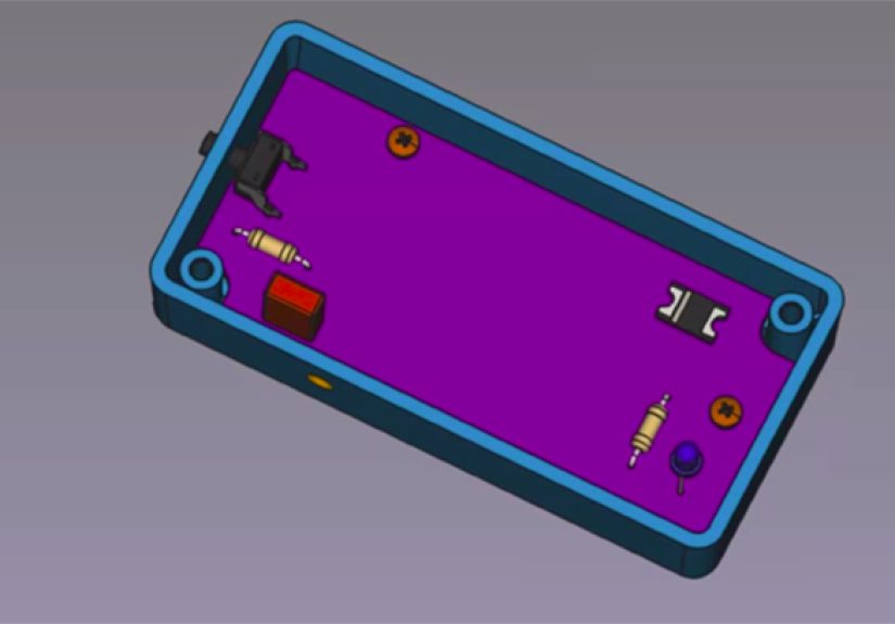
Specific Example: A Small Sensor Board in an Enclosure
Imagine a compact environmental sensor board with USB-C power, a reset button, two LEDs, a temperature sensor, and four mounting holes. The enclosure has a front panel with a USB opening, two light pipes, and a recessed button. In KiCad, the USB-C connector should be placed using exact coordinates from the mechanical design. The LEDs should align with the light pipes, and the reset switch should sit at the correct height for the button plunger. Mounting holes should match the enclosure bosses, with copper keepouts for screw heads.
After adding STEP models for the USB connector, switch, LEDs, and large components, export the assembly as a STEP file. In MCAD, check whether the USB shell aligns with the cutout, whether the reset button has enough travel, whether the enclosure lid clears the tallest component, and whether the screwdriver can reach the screws. This simple review can prevent the most irritating prototype failure: a board that works perfectly until you try to put it in the box.
Experiences From Real KiCad Mechanical Integration Work
One of the most useful lessons from working with KiCad is that mechanical integration should begin before the schematic feels “done.” That sounds backward until you have designed a beautiful PCB and then discover the enclosure has a molded post exactly where your microcontroller lives. In practice, I like to place the immovable objects first: connectors, mounting holes, switches, displays, antennas, heat sources, and anything that touches the outside world. Once those are locked, the rest of the layout has a realistic playground.
Another experience: the 3D viewer is not just for screenshots. It is a debugging tool. I have seen 3D models reveal reversed connectors, wrong package heights, missing components, and models that were scaled in inches when the board expected millimeters. The 2D view may look calm and professional while the 3D view is waving a red flag and shouting, “Your inductor is taller than the enclosure.” It is worth opening the 3D viewer after every major placement change.
STEP export also becomes more valuable when it is done repeatedly. Waiting until the design is finished is risky. A better rhythm is to export a preliminary board when fixed components are placed, another after routing begins, and a final version before fabrication. This lets the mechanical team design around the real board instead of a placeholder block. It also gives both sides time to negotiate changes without turning the final week into an email thunderstorm.
Project organization matters more than people expect. Keep custom footprints, 3D models, and mechanical references in predictable folders. Use clear names such as USB_C_Receptacle.step, Enclosure_Clearance_Model.step, or Board_Outline_RevB.dxf. Avoid mysterious files named final_final_use_this_one_v7.step. Future you deserves better. So does the person who inherits the project six months later and has to figure out why the battery holder is floating 12 mm above the board.
Finally, the most successful KiCad mechanical integrations happen when electrical and mechanical designers talk early. A five-minute conversation about connector height can save a board spin. A shared screenshot of the 3D assembly can prevent a bad enclosure cutout. A quick check of mounting screw clearance can stop copper from ending up under a washer. KiCad gives you the tools, but the workflow succeeds when the team uses them before the prototype becomes a very expensive measuring device.
Conclusion
Mechanical integration with KiCad is not a luxury step reserved for fancy product teams. It is a practical part of designing PCBs that fit, assemble, cool, connect, and survive real-world use. By controlling the board outline, placing mechanical features early, using accurate 3D models, exporting STEP files, and collaborating with MCAD tools such as FreeCAD, Fusion, Onshape, or SOLIDWORKS, you can turn KiCad from a PCB layout tool into a dependable bridge between electronics and physical product design.
The main idea is simple: do not wait until manufacturing to discover mechanical problems. Use KiCad’s 3D and export features as early warning systems. Check the board in context. Verify models. Respect tolerances. Keep the mechanical team involved. Your reward is fewer board spins, cleaner assemblies, better enclosures, and a product that does not need to be “lightly modified” with a rotary tool five minutes before a demo.
Note: Always confirm critical dimensions, tolerances, mounting hardware, enclosure clearances, and fabrication limits with your PCB manufacturer and mechanical design team before ordering production boards.